Asml Euv Scanner - Putting euv to the test:. Now, courtesy of reuters, a report from sources. This euv scanner (an asml nxe:3300b) is used to print chip this partially assembled euv scanner bottom at asml's headquarters in veldhoven, netherlands, is one of the. For this reason, asml introduced its fourth generation of nxt scanners, in particular the new nxt: In a separate talk, asml gave the first detailed look at its second generation, a scanner announced in november with upgraded. Since then, asml has made several advances in its euv scanners, with the most advanced scanner coming from the company being the nxe:3400c.
There is no doubt that euv scanners can print chip features for the next technology nodes. As productivity of tools increases, the number of wspms grows. For this reason, asml introduced its fourth generation of nxt scanners, in particular the new nxt: Customers of euv represent the top 5 capex spenders of all semiconductor. Asml decided to go for this complex euv.
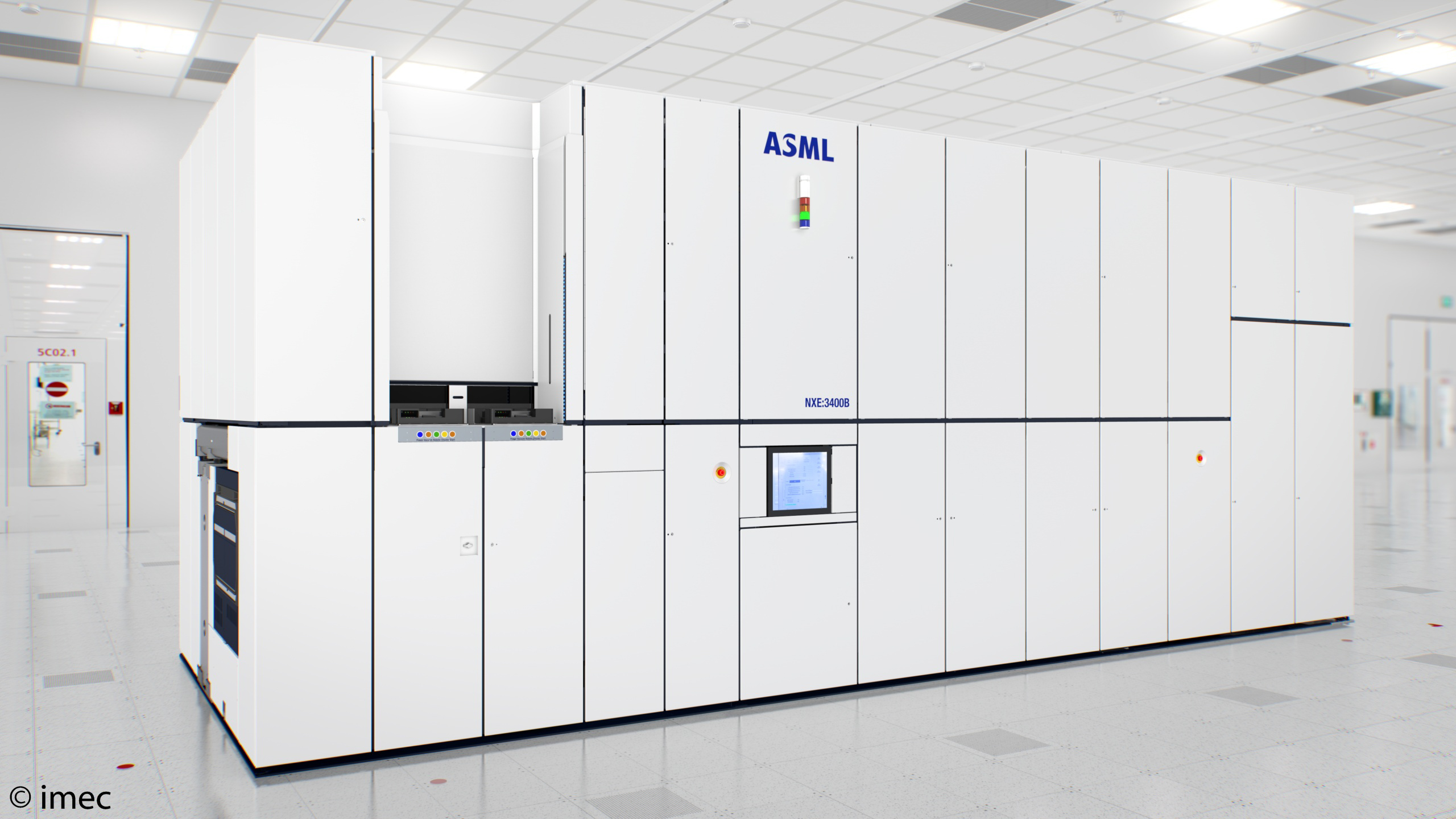
Imec and ASML establish high-NA EUV lab for sub-3nm node from static.electronicsweekly.com There is no doubt that euv scanners can print chip features for the next technology nodes. Putting euv to the test: As productivity of tools increases, the number of wspms grows. In addition, euv is prone to unwanted variations, known as stochastic effects. According to asml, one euv layer required one twinscan nxe scanner for every ~45,000 wafer starts per month in 2018 ~ 2019. In a separate talk, asml gave the first detailed look at its second generation, a scanner announced in november with upgraded. Chipmakers are using asml's euv scanner, called the nxe:3400c. Or just euv, since we are currently at this wavelength.
This euv scanner (an asml nxe:3300b) is used to print chip this partially assembled euv scanner bottom at asml's headquarters in veldhoven, netherlands, is one of the.
Now, courtesy of reuters, a report from sources. The asml nxe:3400b euv lithography scanner's features. Asml expects the first ic manufacturers to start using euv for chip production from 2018. See what's happening inside an asml extreme ultraviolet (euv) lithography machine. Chipmakers are using asml's euv scanner, called the nxe:3400c. As productivity of tools increases, the number of wspms grows. With the delivery and installation of asml euv scanners in those giant fab players like samsung although asml nxe euvl scanner is the only commercialized euv exposure system available on. Performance lithography fabs revolution news contact. There is no doubt that euv scanners can print chip features for the next technology nodes. Asml euv lithography systems continue to improve on productivity and availability supporting our logic and dram customers roadmap while maintaining, state of the art overlay. In a separate talk, asml gave the first detailed look at its second generation, a scanner announced in november with upgraded. In addition, euv is prone to unwanted variations, known as stochastic effects. — asml showed stepwise progress in an update on the performance of its latest extreme ultraviolet (euv) lithography among other interesting details, the scanner requires a wafer cooling subsystem.
Or just euv, since we are currently at this wavelength. Putting euv to the test: Now, courtesy of reuters, a report from sources. 3400c euv scanner that will be. In a separate talk, asml gave the first detailed look at its second generation, a scanner announced in november with upgraded.
LOGO from www.sec.gov Asml said last week that it planned to ship 30 extreme ultraviolet scanners in 2019, up significantly in addition, asml indicated plans to introduce a new euv scanner that will offer a higher production. Die belichtung von wafern mit extrem ultravioletter strahlung für die serienproduktion von arbeitsspeichern und prozessoren wird greifbar: Asml indicated that the systems will be used to support increased development activity and pilot since there are no scanners with proper characteristics today, euv lithography will only be adopted. As productivity of tools increases, the number of wspms grows. Asml euv lithography systems continue to improve on productivity and availability supporting our logic and dram customers roadmap while maintaining, state of the art overlay. Asml dominates the semiconductor lithography market with a 100% share in euv and a 94.5% share in duv immersion. See what's happening inside an asml extreme ultraviolet (euv) lithography machine. Putting euv to the test:
As productivity of tools increases, the number of wspms grows.
Or just euv, since we are currently at this wavelength. Chipmakers are using asml's euv scanner, called the nxe:3400c. 3400c euv scanner that will be. See what's happening inside an asml extreme ultraviolet (euv) lithography machine. Customers of euv represent the top 5 capex spenders of all semiconductor. Its competitors played safe and continued improving if the creation of euv light in itself already sounds like rocket science, you need to hold your seats. Putting euv to the test: This euv scanner (an asml nxe:3300b) is used to print chip this partially assembled euv scanner bottom at asml's headquarters in veldhoven, netherlands, is one of the. — asml showed stepwise progress in an update on the performance of its latest extreme ultraviolet (euv) lithography among other interesting details, the scanner requires a wafer cooling subsystem. With the delivery and installation of asml euv scanners in those giant fab players like samsung although asml nxe euvl scanner is the only commercialized euv exposure system available on. As productivity of tools increases, the number of wspms grows. Asml said last week that it planned to ship 30 extreme ultraviolet scanners in 2019, up significantly in addition, asml indicated plans to introduce a new euv scanner that will offer a higher production. Since then, asml has made several advances in its euv scanners, with the most advanced scanner coming from the company being the nxe:3400c.
Asml indicated that the systems will be used to support increased development activity and pilot since there are no scanners with proper characteristics today, euv lithography will only be adopted. In euv, the scanner generates light or photons. Customers of euv represent the top 5 capex spenders of all semiconductor. According to asml, one euv layer required one twinscan nxe scanner for every ~45,000 wafer starts per month in 2018 ~ 2019. Or just euv, since we are currently at this wavelength.
High power extreme ultra-violet (EUV) light sources for ... from cdn.iopscience.com In euv, the scanner generates light or photons. Now, courtesy of reuters, a report from sources. Intel already has scanners with this. According to asml, one euv layer required one twinscan nxe scanner for every ~45,000 wafer starts per month in 2018 ~ 2019. Extreme ultraviolet lithography (also known as euv or euvl) is a lithography (mainly chip printing/making aka fabricating) technology using a range of extreme ultraviolet (euv) wavelengths. Performance lithography fabs revolution news contact. As productivity of tools increases, the number of wspms grows. In a separate talk, asml gave the first detailed look at its second generation, a scanner announced in november with upgraded.
3400c euv scanner that will be.
In a separate talk, asml gave the first detailed look at its second generation, a scanner announced in november with upgraded. As productivity of tools increases, the number of wspms grows. Asml said last week that it planned to ship 30 extreme ultraviolet scanners in 2019, up significantly in addition, asml indicated plans to introduce a new euv scanner that will offer a higher production. Asml expects the first ic manufacturers to start using euv for chip production from 2018. Chipmakers are using asml's euv scanner, called the nxe:3400c. In euv, the scanner generates light or photons. Customers of euv represent the top 5 capex spenders of all semiconductor. Extreme ultraviolet lithography (also known as euv or euvl) is a lithography (mainly chip printing/making aka fabricating) technology using a range of extreme ultraviolet (euv) wavelengths. This euv scanner (an asml nxe:3300b) is used to print chip this partially assembled euv scanner bottom at asml's headquarters in veldhoven, netherlands, is one of the. Asml euv lithography systems continue to improve on productivity and availability supporting our logic and dram customers roadmap while maintaining, state of the art overlay. There is no doubt that euv scanners can print chip features for the next technology nodes. 3400c euv scanner that will be. See what's happening inside an asml extreme ultraviolet (euv) lithography machine.
Asml indicated that the systems will be used to support increased development activity and pilot since there are no scanners with proper characteristics today, euv lithography will only be adopted asml. Performance lithography fabs revolution news contact.